
CoWoS Packaging Capacity Doubles in 2026, Yet Supply Gap Remains
In 2026, the semiconductor industry hit a milestone that would have seemed ambitious only a few years ago: the global capacity for chip-on-wafer-on-substrate, or CoWoS, advanced packaging roughly doubled. By any traditional metric, that should have eased the pressure on cutting-edge compute supply. Yet, in practice, the opposite is happening. Despite this dramatic expansion, demand for CoWoS capacity still outstrips supply, and the gap is reshaping strategies across the semiconductor ecosystem.
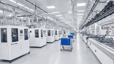
This paradox tells us something profound about where the industry is headed. As artificial intelligence, high performance computing, and data-intensive applications accelerate, the bottleneck is no longer just transistor scaling on a single die. It has shifted into the realm of advanced packaging and heterogeneous integration, where multiple chips are brought together into tightly coupled systems. CoWoS sits at the center of this shift, and its strained capacity acts as a real-time barometer of how quickly the world is trying to build the next generation of computing infrastructure.
From Transistor Scaling to System Scaling
For decades, semiconductor progress was driven primarily by Moore’s Law: shrinking transistors, integrating more functionality into a single monolithic die, and using that density to boost performance and lower cost. As physical and economic limits on scaling emerged, the industry transitioned from a mindset of “bigger chips for more performance” toward “more chips working together as one system.” That transition is the essence of heterogeneous integration.
Heterogeneous integration means combining multiple dies, often from different process nodes and sometimes from different vendors, into a single package. Logic, memory, I/O, analog, RF, and accelerators can all be mixed and matched. Rather than forcing everything onto the most advanced and expensive node, designers can reserve the bleeding-edge processes for compute-intensive logic and use mature nodes for memory, analog, or interface functions. The glue that makes this possible is advanced packaging, and CoWoS is one of its flagship technologies.
What CoWoS Really Is
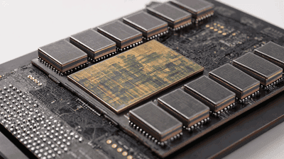
CoWoS, short for chip on wafer on substrate, is a 2.5D advanced packaging scheme that allows multiple large dies to be placed side-by-side on a silicon interposer, which is then attached to an organic substrate. Instead of connecting chips through long PCB traces or conventional packages, CoWoS uses dense, short interconnects on the interposer to achieve much higher bandwidth and lower latency communication between dies. That makes it ideal for high bandwidth memory, or HBM, stacks bonded next to large compute dies such as GPUs, AI accelerators, or high performance CPUs.
In a typical CoWoS package, you might see several HBM stacks surrounding a large logic die, all mounted on a passive silicon interposer. The interposer itself acts like a micro-scale wiring board, hosting thousands of fine-pitch connections between the logic and memory. Compared to standard packages, the result is a massive improvement in data throughput and energy efficiency per bit transferred. This is crucial for AI and high performance computing workloads where data movement, not computation, increasingly dominates energy and performance budgets.
Because CoWoS enables extremely wide memory interfaces and tight logic-memory coupling, it has become the de facto packaging solution for the highest-end AI accelerators and GPUs used in training large models and running demanding inference workloads. Cloud providers, hyperscalers, and AI startups all depend on CoWoS-based parts to deliver the performance needed for modern AI workloads. That dependency, in turn, drives intense demand for CoWoS capacity at leading foundries and outsourced assembly and test providers.
Why Capacity Needed to Double
The surge in AI adoption over the past few years has created a tidal wave of demand at every level of the compute stack. Training large language models, recommendation systems, and generative AI engines now requires racks of accelerators, each packed with multiple HBM stacks. A single advanced GPU might incorporate several HBM stacks on a CoWoS interposer, and a single server may contain multiple such GPUs. Data centers then deploy thousands or tens of thousands of servers.
The multiplier effect is dramatic. A small increase in the number of AI training runs, the complexity of models, or the scale of deployed inference can translate into a huge increase in the number of CoWoS packages required. As AI becomes central not only to internet services but also to enterprises, scientific computing, climate modeling, and even edge applications, demand for these advanced packages has grown much faster than initially forecast.
At the same time, leading chipmakers have aggressively ramped their most advanced process nodes for AI and high performance computing chips. However, those chips cannot deliver their full potential without high bandwidth memory and advanced packaging. This has made CoWoS a critical link in the supply chain. When the industry doubled CoWoS capacity in 2026, it was not an act of luxury; it was an attempt to catch up with a demand curve that had already accelerated beyond expectations.
The Supply Gap: Why Doubling Is Not Enough
The enduring supply gap, even after a doubling of capacity, can be traced to several interlocking factors. First, demand for AI accelerators has not just grown linearly; it has grown in waves, triggered by major software breakthroughs, new model architectures, and the competitive drive among leading cloud and AI companies. Every jump in model size and complexity translates directly into more compute and memory bandwidth requirements, which in turn drive more CoWoS-based systems.
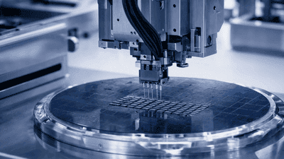
Second, CoWoS manufacturing is inherently complex. It involves multiple precise steps: fabricating large silicon interposers, thinning wafers, accurately placing multiple dies with tight alignment tolerances, managing thermal and mechanical stress, and ensuring high yields across the entire package. Each of these steps has constraints on equipment, materials, and process time. Capacity expansions are not as simple as adding another line of conventional packaging tools; they require specialized equipment, cleanroom space, and process expertise that can take years to ramp.
Third, supply chain constraints extend beyond the packaging facility itself. CoWoS relies on a steady supply of high quality silicon interposers, advanced substrates, and HBM stacks. Any bottleneck in these upstream components can limit the effective CoWoS output even if nominal packaging capacity has doubled. A shortage of HBM, for example, can leave CoWoS lines underutilized or force production prioritization toward certain products and customers.
Finally, demand is concentrated at the very leading edge. While overall packaging capacity may be growing, the portion that meets the strict requirements of the latest AI accelerators is much smaller and harder to expand. Customers want the combination of advanced nodes, high HBM channel counts, large interposers, and tight power and thermal envelopes. These high complexity packages stress every dimension of the CoWoS process, making it harder to achieve both high yields and rapid volume increases.
CoWoS in the Context of Heterogeneous Integration
To understand why CoWoS demand remains so intense, it helps to place it within the broader landscape of heterogeneous integration technologies. CoWoS is part of a growing toolbox that includes fan-out wafer level packaging, 2.5D interposer-based solutions, and true 3D integration such as hybrid bonding. All of these architectures share the goal of building systems from multiple chiplets or dies, but they approach it with different trade-offs in complexity, cost, performance, and density.
In many ways, CoWoS has emerged as the workhorse for high performance logic plus HBM solutions. It provides a relatively mature and well-understood path to connect large logic dies with several memory stacks using a full silicon interposer. Compared to some newer technologies, CoWoS offers a combination of reliability, electrical performance, and manufacturability that makes it attractive for mission-critical data center applications. Designers can pack more transistors into their systems not by growing a single massive die, but by assembling multiple dies on an interposer and letting them communicate at near on-die bandwidths.
Heterogeneous integration also allows innovation at the package level. Chip providers are increasingly building product families around modular chiplets: compute tiles, I/O tiles, accelerator tiles, and memory tiles that can be mixed and matched. CoWoS can act as the foundational platform to bring these chiplets together into tailored solutions for specific workloads. This modularity is one reason why demand for advanced packaging is likely to remain strong even as individual chip designs evolve. The packaging platform becomes a central part of the product strategy.
Technical and Operational Limits on CoWoS Expansion
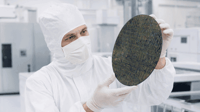
If CoWoS is so vital, why can the industry not simply continue doubling capacity until demand is satisfied? The answer lies in both technical and economic realities. On the technical side, scaling CoWoS capacity involves pushing against several boundaries at once: interposer size and yield, bump pitch, thermal dissipation, and the mechanical integrity of large, complex packages. The larger the interposer and the more dies in the package, the harder it becomes to maintain high yield across the entire assembly.
Yield challenges are particularly acute when integrating very large compute dies and multiple HBM stacks. A defect in any one of these components can render the entire package unusable. Advanced test and known good die strategies can mitigate this risk, but they add complexity and cost. Manufacturers must balance how aggressively they push interposer size and die counts against the risk of yield loss. In practice, that often means capacity expansions cannot be achieved simply by scaling up to ever larger packages; process refinements and design optimizations are needed.
On the operational side, advanced packaging lines require substantial capital investment and highly specialized talent. Building new CoWoS facilities or retrofitting existing ones takes years, not months. Equipment lead times can be long, training staff to run and maintain complex processes is nontrivial, and qualification cycles with major customers are rigorous. All of this slows the rate at which “paper capacity” turns into “usable, high yield capacity” for the most demanding products.
These constraints mean that even a headline figure like “capacity doubled” must be interpreted carefully. The effective capacity available for the highest end AI packages may be much lower than the aggregate number suggests. Yield learning curves, product mix, and prioritization among customers all influence how much actual supply reaches the market at any given time.
Economic and Strategic Implications
The persistent CoWoS supply gap has several economic implications. First, it contributes to premium pricing for leading AI accelerators and HBM-based solutions. When capacity is constrained, suppliers can command higher margins, and access to advanced packaging becomes a competitive differentiator. For hyperscalers and system integrators, securing a reliable pipeline of CoWoS-packaged parts becomes as strategic as negotiating wafer supply at leading process nodes.
Second, it influences product roadmaps and architectural decisions. If a company anticipates limited access to CoWoS capacity, it may design products that use alternative packaging schemes or reduce dependence on ultra-large interposers. Some may pursue multi-node or multi-vendor strategies, where parts of the system are manufactured and packaged through different partners to diversify risk. Others may invest in co-development with foundries and OSATs to secure dedicated capacity for their flagship products.
Third, the supply gap reinforces geographic and ecosystem considerations. Companies may be more inclined to work with packaging partners located in specific regions for reasons of logistics, policy, or resilience. Governments, recognizing that advanced packaging is a strategic technology, may include CoWoS and related capabilities in their industrial policy and incentive programs. This can accelerate new capacity in some regions while leaving others reliant on imports.
Alternative Advanced Packaging Paths
While CoWoS is a central pillar of advanced packaging today, it is not the only path to heterogeneous integration. Other advanced packaging approaches are being developed and scaled to alleviate pressure on CoWoS capacity and provide different trade-offs. Fan-out wafer level packaging, for example, can integrate multiple dies in a planar configuration without a silicon interposer, relying instead on redistribution layers built directly into the package. This can offer attractive cost and form factor benefits for certain applications, though it may not yet match CoWoS for the highest bandwidth requirements.
Another direction is 3D integration using hybrid bonding or through-silicon vias, where dies are stacked vertically and connected with fine-pitch interconnects. This approach can achieve even higher integration density and potentially lower energy per bit than 2.5D interposers. However, 3D integration introduces its own set of challenges in heat removal, design complexity, and testability. For the moment, 2.5D CoWoS-style solutions remain the primary platform for high performance logic plus HBM, while 3D integration is ramping gradually.
These alternative packaging flows provide important relief valves and future options, but they also underscore the central theme of 2026: advanced packaging as a whole, not just wafer fabrication, has become a critical bottleneck. Whether it is CoWoS, fan-out, or 3D stacking, the ability to combine multiple dies efficiently and reliably is now a core determinant of system capability.
Design Strategies in a Constrained CoWoS World
For chip designers and system architects, the persistent CoWoS supply gap forces practical choices. One strategy is to optimize die partitioning and chiplet architectures to make more efficient use of limited interposer real estate. For example, instead of designing a single giant compute die, architects may split functionality across several smaller chiplets that share an interposer. This can improve yield and flexibility while still benefiting from high bandwidth interconnects.
Another strategy is to explore hybrid packaging solutions that mix CoWoS with other technologies. A system might use CoWoS for the most bandwidth-critical components, such as GPU-to-HBM connections, while employing other packaging for less demanding subsystems. This tiered approach can reduce reliance on the most constrained resources while still delivering strong overall performance.
Additionally, close co-design of silicon and packaging becomes more important. Thermal management, power delivery, and mechanical stress all need to be considered holistically. A package that looks optimal in a purely electrical sense may be impractical to manufacture or may suffer from reliability issues. By treating the package as an integral part of the system design from the outset, companies can avoid late-stage surprises and improve the odds that their products can be manufactured at scale within the constraints of available CoWoS capacity.
The Road Ahead: Beyond 2026
Looking beyond 2026, the trajectory of CoWoS and advanced packaging suggests that the industry is still in the early stages of this transformation. Capacity will continue to expand, and yields will improve as processes mature. New materials, smarter thermal solutions, and refined design methodologies will all contribute to more robust CoWoS platforms. However, demand is also poised to grow as AI, exascale computing, and data-intensive applications proliferate across industries.
At the same time, heterogeneous integration will diversify. We can expect more widespread adoption of chiplet-based architectures, standardized interconnect protocols between dies, and innovative combinations of logic, memory, and specialized accelerators. Advanced packaging will not be a monolithic technology but a spectrum of options, each optimized for specific performance, cost, and form factor targets. CoWoS will remain a cornerstone for certain high-end applications, but it will share the stage with a variety of other techniques.
One likely outcome is that the perceived “supply gap” for advanced packaging never fully disappears in the traditional sense. As soon as capacity catches up to one wave of demand, a new wave of innovation and application growth will arrive, stretching the system again. This is not a sign of failure; it is a sign that packaging has become a dynamic, innovation-driven part of the semiconductor value chain rather than a static back-end commodity.
Conclusion: CoWoS as a Signal, Not Just a Technology
The doubling of CoWoS packaging capacity in 2026, combined with the persistent supply gap, is more than a story about manufacturing throughput. It is a signal that the center of gravity in semiconductor innovation has shifted. Advanced packaging and heterogeneous integration now sit alongside lithography and device scaling as foundational enablers of progress. The ability to combine multiple dies into cohesive, high-performance systems has become a key source of competitive advantage.
For chipmakers, system designers, and data center operators, this means that packaging strategies must be elevated to the same level of strategic planning as process node selection and architectural design. Securing access to advanced packaging capacity, co-developing solutions with packaging partners, and designing products that make efficient use of these capabilities will be essential to meeting the exploding demand for compute in the AI era.
For the broader industry, the CoWoS capacity crunch is a reminder that bottlenecks can emerge in unexpected places when technology paradigms shift. The focus is no longer solely on how small we can make a transistor, but on how intelligently we can integrate diverse components into powerful, efficient systems. In that world, CoWoS and its advanced packaging peers are not merely manufacturing steps at the end of the line. They are where the future of heterogeneous integration becomes real.
You May Like

Narrowing Spread Between NAND Spot and Contract Prices in 2026 – A Signal
By 2026, one of the most watched metrics in the NAND flash market has started to shift in a subtle but meaningful way: the spread between spot prices and long‑term contract prices is narrowing. For casual observers, this may look like just another incremental change in a notoriously volatile industry. For memory makers, module houses, device OEMs, and data center buyers, however, a tightening gap between spot and contract prices is a signal—a reflection of evolving supply–demand balance, risk perceptions, and strategic behavior on both sides of the market.

Price Divergence Trading Strategies Between NAND Flash and DRAM ETFs
NAND flash and DRAM sit at the core of AI storage and computing power. Both are memory, but they are not the same business. DRAM is main memory—fast, volatile, and central to high‑bandwidth workloads like AI training and inference. NAND is non‑volatile storage—slower than DRAM, but crucial to persistent data and large‑scale object storage. The cycles that drive their pricing and margins overlap, yet they often diverge. That divergence is where trading strategies between NAND and DRAM ETFs become interesting.

China’s HBM Localization Progress: The Catch-Up Pace of CXMT and XMC
China’s drive to localize advanced memory technologies has accelerated over the past several years. High-Bandwidth Memory (HBM) sits near the center of that strategy because it is integral to AI accelerators, high-performance computing (HPC) and other strategic compute platforms. Two domestic players—ChangXin Memory Technologies (CXMT) and XMC (Xianghui Memory, commonly referred to as XMC)—have become focal points in assessing how quickly China can close the gap with international incumbents on HBM die, stacking, and packaging.

Thermal Simulation Challenges and Solutions in 3DIC AI Chip Design
As AI workloads push chips to deliver ever higher compute density, designers are increasingly turning to three‑dimensional integration (3DIC) to stack dies vertically and pack more functionality into limited footprints. While 3DIC architectures unlock significant performance and bandwidth advantages, they also introduce complex thermal behaviors that are far harder to predict and manage than in traditional 2D layouts.

An Attempt at Compiling a Memory+Compute Fusion Thematic Index – A Dual-Track Framework
Most AI investors talk about “compute” as if it were the whole story: GPUs, accelerators, chips, cores. But every one of those cores needs somewhere to read from and write to. Memory and storage define how wide the data highway really is. In practice, AI performance is a fusion of compute and memory, not a solo act. So why do so many indices and ETFs separate them into different silos—one for semiconductors, one for memory, one for data centers—when the actual workloads keep blending them?
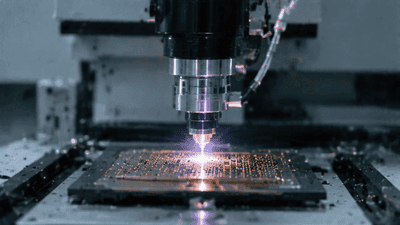
Surging Demand for Laser Drilling and Plasma Dicing Equipment in Advanced Packaging
Advanced packaging has become one of the semiconductor industry’s most important growth engines, and it is now pulling a surprising set of process tools into the spotlight. Among the most in-demand are laser drilling and plasma dicing equipment. These machines sit close to the heart of heterogeneous integration, fan-out packaging, wafer thinning, TSV formation, glass substrate processing, and other advanced flows where precision, yield, and throughput matter enormously. As packaging moves from a back-end afterthought to a strategic platform, the equipment used to shape, open, and separate materials has become just as important as the dies themselves.

D2D Interface Bandwidth and Latency Comparison in Chiplet Architectures
Chiplet architecture has turned the package into a real performance battleground. Once multiple dies are placed side by side or stacked within the same advanced package, the quality of the die-to-die, or D2D, interface becomes one of the most important determinants of system behavior. Bandwidth is no longer a nice-to-have metric, and latency is no longer a small implementation detail. Together, they shape whether a chiplet system feels nearly monolithic or frustratingly fragmented.

Stock Selection Logic and Alpha Validation of ESG-Themed Semi ETFs
Semiconductor themed ETFs are no longer just about growth and cycles. A growing subset now layers environmental, social, and governance (ESG) criteria on top of traditional sector exposure. These ESG semi ETFs promise two things at once: access to one of the market’s most powerful secular themes, and alignment with sustainability and governance standards. The pitch is appealing, but it raises two hard questions. First, how exactly are these stocks being selected? Second, does the ESG overlay help, hurt, or leave alpha unchanged?